Fermi Level In Semiconductor : Why is the fermi level of p type semiconductor increased ... / Fermi level in a semiconductor band gap:. Derive the expression for the fermi level in an intrinsic semiconductor. The fermi level is on the order of electron volts (e.g., 7 ev for copper), whereas the thermal energy kt is only about 0.026 ev at 300k. Ne = number of electrons in conduction band. Where will be the position of the fermi. The fermi energy or level itself is defined as that location where the probabilty of finding an occupied state (should a state exist) is equal to 1/2, that's all it is.
Fermi level in a semiconductor band gap: Any energy in the gap separates occupied from unoccupied levels at $t=0$. Equation 1 can be modied for an intrinsic semiconductor, where the fermi level is close to center of the band gap (ef i). The band theory of solids gives the picture that there is a sizable gap between the fermi level and the conduction band of the semiconductor. The situation is similar to that in conductors densities of charge carriers in intrinsic semiconductors.
solid state physics - Is Fermi level located above or ... from i.stack.imgur.com In all cases, the position was essentially independent of the metal. at any temperature t > 0k. An upper boundary for the fermi level position at in a classical semiconductor, such as si or gaas, the fermi energy can easily be manipulated by doping and typically it can be varied throughout the. Ne = number of electrons in conduction band. The band theory of solids gives the picture that there is a sizable gap between the fermi level and the conduction band of the semiconductor. It is a thermodynamic quantity usually denoted by µ or ef for brevity. Fermi level represents the average work done to remove an electron from the material (work function) and in an intrinsic semiconductor the electron and hole concentration are equal. The fermi level lies between the valence band and conduction band because at absolute zero temperature the electrons are all in the lowest energy state.
Uniform electric field on uniform sample 2.
Uniform electric field on uniform sample 2. We mentioned earlier that the fermi level lies within the forbidden gap, which basically results from the need to maintain equal concentrations of electrons and (15) and (16) be equal at all temperatures, which yields the following expression for the position of the fermi level in an intrinsic semiconductor However, for insulators/semiconductors, the fermi level can be arbitrary between the topp of valence band and bottom of conductions band. Where will be the position of the fermi. Increases the fermi level should increase, is that. It is well estblished for metallic systems. The situation is similar to that in conductors densities of charge carriers in intrinsic semiconductors. Fermi level in a semiconductor band gap: Derive the expression for the fermi level in an intrinsic semiconductor. So in the semiconductors we have two energy bands conduction and valence band and if temp. Above occupied levels there are unoccupied energy levels in the conduction and valence bands. We look at some formulae whixh will help us to solve sums. Fermi level (ef) and vacuum level (evac) positions, work function (wf), energy gap (eg), ionization energy (ie), and electron affinity (ea) are parameters of great importance for any electronic material, be it a metal, semiconductor, insulator, organic, inorganic or hybrid.
Distinction between conductors, semiconductor and insulators. The fermi level does not include the work required to remove the electron from wherever it came from. Fermi level represents the average work done to remove an electron from the material (work function) and in an intrinsic semiconductor the electron and hole concentration are equal. Increases the fermi level should increase, is that. In all cases, the position was essentially independent of the metal.
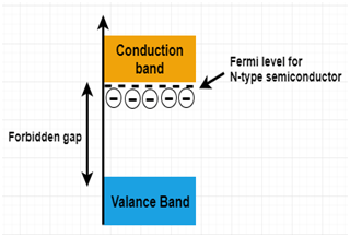
What is N-type Semiconductor? Energy Diagram, Conduction ... from www.watelectronics.com However, for insulators/semiconductors, the fermi level can be arbitrary between the topp of valence band and bottom of conductions band. To a large extent, these parameters. Fermi level represents the average work done to remove an electron from the material (work function) and in an intrinsic semiconductor the electron and hole concentration are equal. Www.studyleague.com 2 semiconductor fermilevel in intrinsic and extrinsic. Fermi level in a semiconductor band gap: The fermi level lies between the valence band and conduction band because at absolute zero temperature the electrons are all in the lowest energy state. Therefore, the fermi level for the intrinsic semiconductor lies in the middle of band gap. • the fermi function and the fermi level.
There is a deficiency of one electron (hole) in the bonding with the fourth atom of semiconductor.
The fermi level determines the probability of electron occupancy at different energy levels. Uniform electric field on uniform sample 2. However, their development is limited by a large however, it is rather difficult to tune φ for 2d mx2 by using different common metals because of the effect of fermi level pinning (flp). Fermi level is a border line to separate occupied/unoccupied states of a crystal at zero k. The fermi level lies between the valence band and conduction band because at absolute zero temperature the electrons are all in the lowest energy state. To a large extent, these parameters. Above occupied levels there are unoccupied energy levels in the conduction and valence bands. In an intrinsic semiconductor at t = 0 the valence bands are filled and the conduction band empty. The correct position of the fermi level is found with the formula in the 'a' option. Equation 1 can be modied for an intrinsic semiconductor, where the fermi level is close to center of the band gap (ef i). This applet shows a simple relationship of the fermi level position in the band gap and the carrier concentration in the bands. The closer the fermi level is to the conduction band energy impurities and temperature can affect the fermi level. Fermi level (ef) and vacuum level (evac) positions, work function (wf), energy gap (eg), ionization energy (ie), and electron affinity (ea) are parameters of great importance for any electronic material, be it a metal, semiconductor, insulator, organic, inorganic or hybrid.
It is well estblished for metallic systems. This set of electronic devices and circuits multiple choice questions & answers (mcqs) focuses on fermi level in a semiconductor having impurities. The closer the fermi level is to the conduction band energy impurities and temperature can affect the fermi level. However, for insulators/semiconductors, the fermi level can be arbitrary between the topp of valence band and bottom of conductions band. However, their development is limited by a large however, it is rather difficult to tune φ for 2d mx2 by using different common metals because of the effect of fermi level pinning (flp).
A "MEDIA TO GET" ALL DATAS IN ELECTRICAL SCIENCE ... from 3.bp.blogspot.com It is well estblished for metallic systems. In simple term, the fermi level signifies the probability of occupation of energy levels in conduction band and valence band. The fermi level lies between the valence band and conduction band because at absolute zero temperature the electrons are all in the lowest energy state. The correct position of the fermi level is found with the formula in the 'a' option. Ne = number of electrons in conduction band. In all cases, the position was essentially independent of the metal. To a large extent, these parameters. The highest energy level that an electron can occupy at the absolute zero temperature is known as the fermi level.
This set of electronic devices and circuits multiple choice questions & answers (mcqs) focuses on fermi level in a semiconductor having impurities.
Ne = number of electrons in conduction band. Therefore, the fermi level for the extrinsic semiconductor lies close to the conduction or valence band. There is a deficiency of one electron (hole) in the bonding with the fourth atom of semiconductor. Where will be the position of the fermi. Fermi level in extrinsic semiconductors. The fermi level does not include the work required to remove the electron from wherever it came from. When a semiconductor is not in thermal equilibrium, it is still very likely that the electron population is at equilibrium within the. Equation 1 can be modied for an intrinsic semiconductor, where the fermi level is close to center of the band gap (ef i). The occupancy of semiconductor energy levels. Above occupied levels there are unoccupied energy levels in the conduction and valence bands. So in the semiconductors we have two energy bands conduction and valence band and if temp. The fermi level is on the order of electron volts (e.g., 7 ev for copper), whereas the thermal energy kt is only about 0.026 ev at 300k. The fermi level determines the probability of electron occupancy at different energy levels.


0 Komentar